
Sep 11,2026
Coarse Grinding vs. Fine Grinding for Semiconductor Wafers
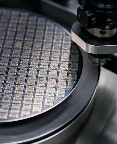
Semiconductor wafer grinding is a mechanical processing step used to remove a controlled amount of material from a wafer surface and achieve the required thickness, flatness, and surface condition. It is widely used in semiconductor wafer processing, particularly for silicon and silicon carbide wafers where dimensional control and surface quality directly affect subsequent manufacturing steps.
Unlike general-purpose grinding, wafer grinding requires close control of material removal and surface damage. The grinding tool, abrasive grit, wheel structure, grinding speed, feed rate, and grinding depth all influence the final result. For this reason, wafer grinding is not simply a matter of removing material as quickly as possible. The process must balance removal efficiency with dimensional accuracy and surface quality.
Semiconductor wafers need to meet specific thickness and surface requirements before they move into subsequent processing stages. Grinding provides a controlled method for removing material and adjusting the wafer to the required dimensions.
One of the main purposes is wafer thickness control. A wafer may need to be reduced from its initial thickness to a target value according to the requirements of the semiconductor device or substrate. Grinding allows material to be removed at a controlled rate rather than relying on a less predictable mechanical process.
Surface condition is another important consideration. Grinding changes the wafer surface through abrasive contact, so the process must be controlled to avoid excessive scratches, grinding marks, chipping, or other forms of surface damage. A grinding process that achieves the correct thickness but leaves unacceptable surface defects cannot be considered successful.
Wafer grinding also contributes to dimensional consistency. For semiconductor applications, small variations in thickness or surface condition can affect later processes, particularly when wafers need to meet tight manufacturing tolerances.
The main purposes of wafer grinding can therefore be summarized as:
These requirements make grinding an important part of semiconductor wafer processing, especially when the process involves high-value wafers where excessive material loss or surface damage can increase manufacturing costs.
The basic principle of wafer grinding is straightforward: an abrasive grinding tool contacts the wafer surface and removes material through controlled mechanical action. In semiconductor applications, however, the actual process requires careful coordination between the wafer, grinding tool, machine, and processing parameters.
The wafer is first positioned and secured on the grinding equipment. The grinding tool then contacts the designated wafer surface while rotating at a controlled speed. Diamond abrasive particles in the grinding tool remove material from the wafer as the tool moves relative to the workpiece.
The amount of material removed depends on several factors, including grinding depth, feed rate, wheel speed, abrasive grit, and the characteristics of the wafer material. Cooling and chip removal also matter because heat and accumulated grinding debris can affect processing stability and surface quality.
For many applications, grinding can be divided into a coarse stage and a fine stage.
| Grinding stage | Main purpose | Main processing focus |
|---|---|---|
| Coarse grinding | Remove material efficiently and reduce wafer thickness | Higher material removal |
| Fine grinding | Refine dimensions and surface condition | Surface quality and controlled removal |
Coarse grinding is generally used when a relatively larger amount of material needs to be removed. Processing efficiency is important at this stage because the main objective is to bring the wafer closer to its target thickness.
Fine grinding follows when tighter control is required. The material removal rate is lower, while greater attention is given to surface condition, thickness accuracy, and the reduction of grinding-related damage.
The distinction between these stages is important because a grinding tool that performs well for high material removal may not necessarily provide the surface condition required for fine grinding. Tool characteristics and processing parameters therefore need to correspond to the specific stage of wafer processing.
For this reason, a wafer grinding process should be considered as a controlled sequence rather than a single operation. The target thickness, wafer material, grinding stage, and required surface condition all influence how the process should be performed.
Different semiconductor materials place different demands on the grinding process. Silicon remains one of the most widely processed wafer materials, while silicon carbide has become increasingly important in applications requiring high-temperature, high-power, or high-frequency performance.
Silicon wafer grinding is used to remove material from silicon wafers and bring them to the required thickness and surface condition. Because silicon wafers are used across a wide range of semiconductor applications, grinding requirements can vary according to wafer size, thickness, processing stage, and subsequent manufacturing requirements.
The grinding process needs to provide controlled material removal without creating excessive surface damage. Abrasive selection and grinding parameters therefore need to be matched to the processing objective.
For high-volume wafer processing, consistency is particularly important. Variations in grinding conditions can lead to differences in wafer thickness, surface roughness, or grinding marks, making stable tool performance an important consideration.
SiC wafer grinding presents a different set of processing challenges. Silicon carbide is significantly harder than conventional silicon, which makes material removal more demanding and places greater requirements on the grinding tool.
The combination of material hardness and the need for controlled surface quality means that the grinding process needs sufficient abrasive performance while maintaining stable operation. Tool sharpness, abrasive grit, heat dissipation, and grinding parameters can all influence the result.
For this reason, silicon carbide wafer grinding should not simply be treated as a harder version of silicon grinding. The material properties of SiC need to be considered when selecting the grinding tool and establishing processing conditions.
A more detailed discussion of the specific challenges associated with SiC grinding can be addressed separately, rather than adding unnecessary material to a general introduction to wafer grinding.
The grinding tool is one of the most important variables in wafer processing because it directly determines how abrasive particles interact with the wafer surface. Diamond-based grinding tools are commonly used where efficient material removal and controlled processing are required.
A wafer grinding disc contains abrasive particles that perform the actual cutting and material removal. The disc structure, abrasive grit, tooth configuration, and other design characteristics affect how the tool behaves during processing.
For semiconductor applications, several tool characteristics are particularly important:
Grit size also needs to match the processing stage. Coarser abrasive configurations can support higher material removal during rough processing, while finer grits are generally associated with applications where surface quality and controlled removal are more important.
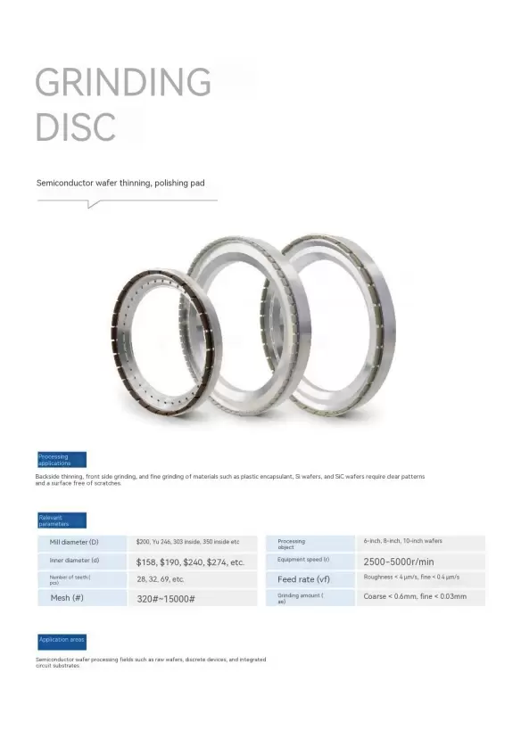
Meijie's Semiconductor Processing solutions include grinding discs designed for wafer processing applications. The available configurations cover different wafer sizes and grinding requirements, including applications involving 6-inch, 8-inch, and 10-inch wafers.
For example, grinding disc specifications can vary in abrasive mesh, tooth configuration, disc dimensions, and operating conditions. These differences are not simply product variations; they allow the tool to be matched to the wafer, equipment, and processing stage.
Tool compatibility is also important. A grinding disc needs to operate properly with the equipment while maintaining stable rotation and feed conditions. Even a high-performance abrasive tool may produce inconsistent results if its structure or operating conditions are not appropriate for the machine.
The right wafer grinding wheel or grinding disc should therefore be selected according to the complete processing requirement rather than abrasive hardness alone.
Wafer grinding quality depends on the interaction between the tool, wafer material, equipment, and processing conditions. Changing one parameter can affect both material removal efficiency and surface quality.
| Factor | Influence on grinding |
|---|---|
| Grit size | Affects material removal and surface finish |
| Grinding speed | Influences processing efficiency and heat generation |
| Feed rate | Affects material removal and surface condition |
| Grinding depth | Influences grinding load and potential surface damage |
| Tool condition | Affects sharpness, stability, and processing consistency |
Grit size is one of the most visible tool-related factors. A suitable abrasive size needs to provide the required material removal without creating unnecessary surface damage. The appropriate choice depends on whether the process is focused on rough material removal or finer surface treatment.
Grinding speed and feed rate also influence the interaction between the abrasive and wafer. Excessive or unsuitable conditions can increase grinding load and heat generation, while overly conservative conditions may reduce processing efficiency.
Grinding depth has a direct relationship with the amount of material removed during each operation. Larger removal amounts can increase the mechanical load on the grinding system, so the depth needs to be appropriate for the material and processing stage.
The condition of the grinding tool matters as well. As abrasive performance changes during use, grinding behavior can change accordingly. Reduced sharpness may affect removal efficiency, surface condition, and overall process stability.
Cooling and chip removal should not be overlooked. Grinding generates heat and produces fine particles from the material being removed. If heat or debris accumulates in the grinding area, it can interfere with stable processing and contribute to surface defects.
These factors should not be considered independently. The same grinding parameters may produce different results when the wafer material, abrasive grit, tool structure, or equipment changes. A stable wafer grinding process therefore depends on matching the complete set of conditions to the specific application.
No. Wafer grinding and polishing are different processes with different primary purposes.
Grinding uses abrasive action to remove material relatively efficiently and is commonly used when wafer thickness needs to be reduced or adjusted. Polishing generally focuses more heavily on refining the surface condition and reducing surface irregularities left by earlier processing.
In practical wafer manufacturing, grinding and polishing can therefore serve complementary roles. Grinding handles controlled material removal, while subsequent finishing processes can further improve the surface when required.
Coarse grinding is primarily concerned with removing material efficiently and bringing the wafer closer to its target thickness. Fine grinding uses more controlled material removal and places greater emphasis on surface quality, dimensional control, and limiting grinding damage.
The two stages may therefore use different grinding conditions and tool configurations. Selecting the appropriate grinding approach depends on the starting wafer condition and the required final result.
Diamond is used because of its high hardness and strong abrasive performance, making diamond-based tools suitable for removing material from demanding wafer materials.
For semiconductor applications, however, abrasive hardness alone is not enough. Tool sharpness, grit size, structure, heat dissipation, chip removal, and equipment compatibility all affect the actual grinding result.
A suitable diamond grinding disc should therefore provide a balance between material removal efficiency, surface quality, and process stability rather than focusing on a single performance characteristic.
Semiconductor wafer grinding is a controlled material-removal process used to achieve the required wafer thickness, surface condition, and dimensional consistency. Its effectiveness depends on more than the grinding machine itself. Wafer material, abrasive characteristics, tool structure, grinding parameters, cooling, and chip removal all contribute to the final result.
For silicon and SiC wafers, the processing requirements can differ significantly, particularly when the material becomes harder and more sensitive to grinding-related damage. Selecting an appropriate diamond grinding tool and matching it with the processing stage is therefore an important part of maintaining stable wafer production.
A clear understanding of the grinding process also makes it easier to evaluate grinding tools based on the actual application rather than specifications alone. For manufacturers working with semiconductor wafers, the focus should remain on the relationship between material removal, surface quality, thickness control, and processing stability.